Advancing microelectronics for high-energy physics
Fermilab is a global leader in developing advanced microelectronics for extreme environments, including high radiation and cryogenic conditions. The lab’s expertise includes application-specific integrated circuit – also known as ASIC – design, sensor and AI co-design and system integration. With state-of-the-art facilities and close collaboration with scientists, Fermilab engineers create high-precision, intelligent instruments that advance high-performance sensing and quantum information science. These efforts support the U.S. Department of Energy’s mission and drive innovation in industries such as space exploration, medical imaging and autonomous vehicles.
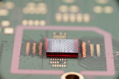
Custom ASIC development for extreme environments
Fermilab’s custom ASIC development is driven by three specialized groups:
- Analog and quantum cryoelectronics: Develops silicon-proven IPs and methodologies for applications such as qubit readout and cryogenic data converters, supporting advancements in quantum computing and sensing technologies.
- High-speed digital design and verification: Specializes in advanced digital ASIC design, verification and AI-on-chip solutions to enable efficient data processing for large-scale endeavors like the Deep Underground Neutrino Experiment and the High-Luminosity Large Hadron Collider.
- Timing and cross-cutting initiatives: Advances precision timing electronics, silicon photonics and superconducting sensor systems to address critical challenges in high-energy physics and dark matter detection.
Together, these groups deliver transformative innovations by integrating cutting-edge technologies with strategic collaborations.
Extreme environment engineering
Fermilab’s designs are both high-performing and resilient, operating in some of the most unforgiving conditions imagined by science. From high-energy particle bombardment to extreme temperatures, Fermilab microelectronics are built to endure decades of reliable operation, ensuring experiments yield results that benefit society.
Pioneering next-generation instruments
Fermilab develops ultraprecise instrumentation that pushes performance boundaries. By integrating high-bandwidth memory, electronics and photonics into heterogeneously designed systems, Fermilab engineers enable efficient, low-latency, energy-efficient data processing. Through co-designing materials, algorithms and circuits, they advance reliability, precision and efficiency, keeping Fermilab at the forefront of scientific and computational innovation.
Supporting the ecosystem for extreme environments
Fermilab engineers lead the development of process design kits optimized for challenging environments, including cryogenic temperatures and high-ionizing radiation. These PDKs, with advanced device models and standard cell libraries, support robust electronics built for decades of reliable operation in inaccessible conditions. By collaborating with academia, government and industry, Fermilab fosters a global ecosystem that drives innovation and shares expertise across fields.
High-throughput testing capabilities
Fermilab offers world-class facilities for testing and characterizing integrated circuits, sensors and electronic systems. Its capabilities include high-throughput automated testing, precision performance analysis and specialized testing for extreme environments such as high radiation and cryogenic conditions. With robotic testing systems and cryogenic platforms, Fermilab ensures reliable performance for both large-scale experiments and custom development needs.
Driving open-source innovation
In collaboration with academic partners, Fermilab is developing open-source hardware-software co-design tools. These tools optimize the implementation of machine learning algorithms on efficient hardware platforms, expanding access to advance technology for small businesses and academic institutions.
Leadership in chip integration
Fermilab has been a pioneer in chip integration technologies, founding the 3D IC Consortium in 2008. This initiative advanced multi-project wafer capabilities for 3D integration, enabling cutting-edge bonding methods such as solid-liquid interdiffusion, Cu-Cu thermocompression, and DBI® hybrid bonding. Today, Fermilab engineers continue to collaborate with industry, nonprofit and academic partners to advance chiplet-based solutions.
Workforce development
Fermilab’s ASIC Design Associate Program gives students hands-on experience in microelectronics research. This tailored internship program helps students transition from summer roles to part-time positions during the academic year, fostering meaningful contributions to chip tape-outs. Fermilab also participates in initiatives like the HEPIC Traineeship Program, SULI and other internships programs, helping develop a steady pipeline of talent across the nation.